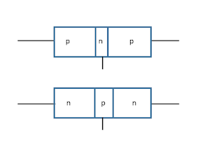
Transistor is a three terminal semiconductor device that are used in electrical/electronic system as a switch, amplifier etc. Generally, transistor is a non-linear semiconductor device which consist of two pn junction and it is more useful as compare to diode (2 terminal semiconductor device). Here we are going to discuss about transistor symbol, npn transistor symbol, pnp transistor symbol. Transistor can be divided into two types, they are [1. Bipolar junction transistor (BJT) 2. Field effect transistor(FET) ]. Generally, when we say transistor that mean it is bipolar junction transistor. BJT transistor is a semiconductor device which is formed by sandwiching n-type material by p-type material or p-type material by n-type material. So transistor can be classified into 2 types i.e. 1. pnp transistor 2. npn transistor
 |
| pnp and npn transistor |
Transistor symbol
The above figure are pnp transistor and npn transistor where it has 3 section of doped semiconductor. Among these 3 section, first one is emitter, middle one is base and last one is collector for both type of transistor. The symbol of transistor is given by: -npn transistor symbol
pnp transistor symbol
As we know, transistor has 3 terminal i.e. 3 parts. They are:-
1. Emitter : - Emitter is always forward biased with respect to base and it is heavily doped. As we can see on figure, emitter is wider than base and thinner than collector. Due to heavily doped, it can inject large number of electros or holes [ holes are majority charge carrier and electros are minority charge carrier for pnp transistor whereas electrons are majority charge carrier and holes are minority charge carrier for npn transistor.] For npn transistor, emitter is n-type and for pnp transistor, emitter is p-type.
2. Base :- Base is the middle part of transistor which is lightly doped and very thin as compared to emitter and collector. The most of charge carrier passes thorough it to the collector. For pnp transistor, base is n-type and for npn transistor, base is p-type.
3. Collector :- Collector is always reversed biased with respect to base and it is moderately doped. For npn transistor, collector is n-type and for pnp transistor, collector is p-type. As compared to base and emitter, it is wider than both base and emitter.
If emitter base junction is forward biased and collector base junction is reversed biased then it is said that transistor is in active mode and acts as amplifier. Similarly, if emitter base junction and collector base junction are forward biased then it is said that transistor is in saturation mode. At saturation mode, it can flow current as switch closed If emitter base junction and collector base junction are in reversed biased, then it is said that the transistor is in cutoff mode. At cutoff mode, current won't flow in the circuit so it acts as open switch. By using cutoff mode and saturation modes of transistor, transistor can be used as switch. Also, if emitter base junction is reversed biased and collector base forward biased junction, this is known as inverse active mode which is used in TTL circuits.
In the transistor, emitter current (IE) is the sum of collector current ( IC ) and base current (IB ) i.e.
IE = IC + IB
This is true relation for both npn transistor and pnp transistor. Also, IB is much lesser as compared to IC so, it can be written as: -
IE ⋍ IC


No comments:
Post a Comment
----Please share your opinion with us-----